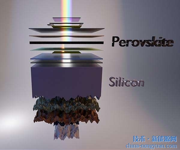
A scientific team at Moscow State University of Electronic Technology has developed a method for producing nanoporous alumina. With this alumina, a series of modern materials including photonic crystals for semiconductor devices can be created. At present, microelectronic semiconductor devices are primarily created by photolithographic techniques. However, photolithography is too expensive, and the series of physical and technical bottles inhibits its development. Therefore, everyone is actively developing methods that are based on self-development. One such method is semiconductor nanopatterning (creating a phenotype with nanoscale elements), ie, plasma etching of a semiconductor and the use of porous anodized aluminum die. Intuitively, the picture on the polymer photographic material is transferred to the corresponding semiconductor structure layer. In this process, the unmodulated region in the polymer material is removed (in fact, this method is called etching). In order to optimize this process, a metal sublayer, in particular a titanium film, is introduced into the alumina mold structure. However, in the scientific literature, there is currently no data available for selecting two-layer hard dies to optimize the structural parameters and control the semiconductor nano-molding process. In order to solve this problem, the scientists of the Moscow National Institute of Electronic Technology, led by AN Belov, studied the process of nano-molding silicon wafers with porous alumina die. The researchers chose a silicon wafer as the substrate and applied a 10-50 nm thick titanium film and a 2 μm thick aluminum film on the substrate by magnetron sputtering. The anodizing of the aluminum film is performed in two steps (anodic oxidation, ie, oxidation of aluminum by electrochemical means for the purpose of forming a metal oxide on the surface thereof) to form a porous alumina mold. Then, the resulting structure was shaped on an argon ion etching apparatus. Through sequence analysis and step-by-step analysis of the structure, the structural state in different stages of the anodization process and the structural state after argon bombardment of the particles were found. The researchers determined the optimal anodization time for establishing an effective hard die for porous alumina, revealing the optimum thickness of the titanium auxiliary sublayer. In addition, they also found that when silicon is plasma-etched through an aluminum oxide die, the depth of etching on the silicon wafer depends on the azimuthal ratio of the alumina pores. In the course of the study, the researchers succeeded in realizing the various conditions for accurately repeating the depth of the aluminum oxide die hole pattern on the silicon wafer when the wafer is nano-patterned. This scientific research and development has been supported by the Russian Federal Special Program for "Innovation in Russian Science and Technology Education Talent."
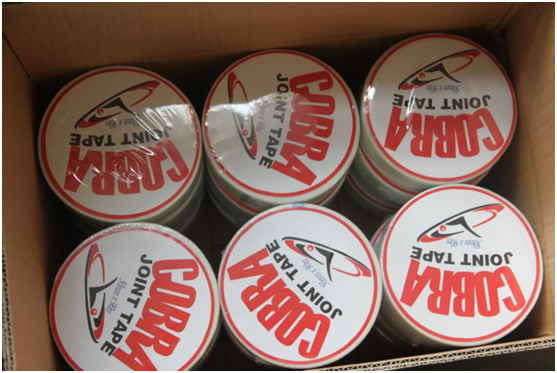
Fiberglass Self-adhesive Joint Tape is made of C-glass or E-glass filament
yarn to weave fiberglass mesh and then treated with high elastic pressure
sensative glue. Characteristics
are high tensile strength, good dimensional stability, stability to
temperature, good elasticity, capillary action, and corrosion resistance.
Fiberglass self-adhesive mesh
tape is
widely used in joining plaster plates, mending drywall cracks and piecing
together and making up different kinds of plates. It goes on faster, adheres
better, and requires no pasting or stapling. It won't tear, shrink, stretch or
bubble, while it hides joints, cracks and holes permanently.
Fiberglass Drywall Joint Tape,Fiberglass Self-adhesive Joint Tape,Drywall Joint Tape,Fiberglass Mesh Tape Yangzhou Jiangdu Chenguang Special Equipment Factory , http://www.siliconebakingmats.com
