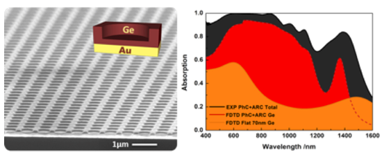
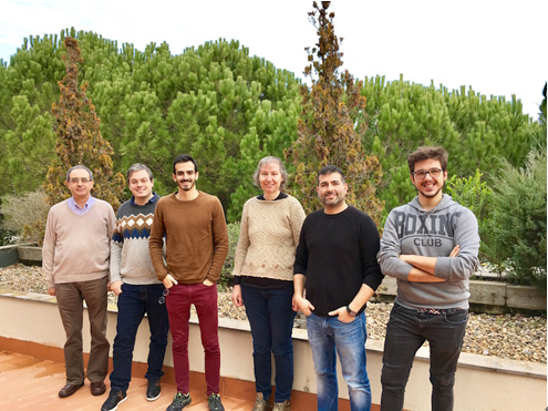
Using nanoimprint lithography, the nanostructured thin layer of semiconductor germanium can greatly increase its light absorption in the visible to near-infrared wavelength range. Broadband absorption comes from the strong interaction between Brewster and the photonic crystal mode in the material, and this effect can greatly promote the development of photovoltaic engineering such as photovoltaics and communications. As shown in the figure: The left picture shows the SEM micrograph of the photonic structure. The inset shows the scheme of a Ge photonic structure on a metal substrate. The graph on the right shows that the absorption of germanium on the gold substrate is 70 nm compared to the absorption of the Ge element surface (black curve) and no anti-reflection coating (red curve). Image source: A Mihi Designing ultra-thin semiconductor materials that absorb light in a range of wavelengths is critical to improving optoelectronic devices to more efficiently convert light into active electrons. One way to achieve this is to increase the thickness of the semiconductor layer so that it captures the largest number of photons across the spectrum. Researchers at the Institute of Materials Research in Barcelona, ​​Spain, have adopted a different approach, using different optical trap strategies, so that they can still absorb light while reducing the amount of semiconductor. In the photon structure they studied, incident light was coupled to different types of optical resonance modes: Brewster and mixed photon-plasma resonance modes. It is these resonances that concentrate the light field in a small volume and allow the material to absorb visible light into the near infrared range (400-1500 nm). é”— interacts with light Agustin Mihi, head of the research team, explained that the Brewster mode is a photon mode in which there is no light reflected from the surface. Due to the high refractive index of the semiconductor and the non-ideal behavior of the precious metal in the visible portion, a thin layer of semiconductor used in our research is on the precious metal substrate to maintain this type of mode spectrum. In this mode, light is strongly confined to the film at wavelengths determined by its thickness. "Because of the nanostructure of the germanium (Ge) film in our sample, light can interact with two effective germanium thicknesses: one is the Brewster mode and the other is the plasma-photon mode. As shown: the research team consists of left and right: Miquel Garriga, Juan Luis GarcÃa-Pomar, Pau Molet, Isabel Alonso, AgustÃnMihi and Cristiano Matricardi. Image source: ICAMB The infrastructure built by the researchers consisted of a two-dimensional array of cylindrical holes built into the gold film using soft lithography. This scalable technology has the advantage of being compatible with large-scale production processes such as rolls. Photon resonance phenomenon of hypersurface “It is very challenging to achieve broadband light absorption through separate photon resonances,†says Mihi, because the light absorption of each resonance amplification works only in a specific wavelength range. In our experiments, we created a slave. Near-infrared to visible light exhibit a series of photonic resonance transition surfaces that increase the light absorption of all energy of the Ge layer above its electron band gap. In fact, broadband absorption comes from simultaneous excitation of different resonances in the entire absorption spectrum of the Ge layer. Mihi said, "In the visible light, our photonic structure maintains a wide Fabry Perot resonance, which is enhanced by coupling with the Brewster mode as described above. In the near infrared Among them, there are multiple absorption peaks from the plasma-photon mode excited in a photonic crystal prepared on a metal substrate. Applications in the field of photovoltaics and communications He added: "Photonic crystals provide a way to couple light in the plane direction of ultra-thin Ge films, enabling them to limit photons of long wavelengths (up to 1400 nm). We have also carefully designed this surface to couple this light to slow Light mode, which combines photonic crystal and plasma effects to produce strong absorption peaks. Such powerful broadband absorption may be useful for manufacturing more efficient photovoltaic devices, especially near-infrared absorption (up to 100% in important telecom windows) can benefit applications such as photodetectors. The research team has published this research in the journal Advanced Materials, and they are now busy using their nanostructured Ge to design different optoelectronic devices. “This includes third-generation solar cells (based on perovskite materials). They hope to effectively increase efficiency and compete with existing silicon technologies.†Guangdong Jishengke Industrial Co., Ltd. , https://www.suronart.com

Nanostructured semiconductors become superabsorbents of light
Abstract Using nanoimprint lithography, the nanostructured thin layer of semiconductor germanium can greatly improve its light absorption in the visible to near-infrared wavelength range. Broadband absorption comes from the strong interaction between Brewster and the photonic crystal mode in the material, and this effect can be...